

Today, Samsung’s LSI has taken the virtual stage to announce its new flagship Exynos 2100. The new chip is quite distinctive to Samsung’s chipset segment because it represents a departure from previous iteration designs – being the first SoC not to use Samsung’s internal performance CPU microarchitecture, but relying instead on Arm’s Cortex cores like the new X1.
It’s a big change for Samsung not just technologically, but also in terms of overall tone and messaging – with more optimistic enthusiasm from the company and also the first launch event ever actually presented to the Samsung Mobile SoC, closely mimicking what we’d like to see from Qualcomm.
The new SoC promises some pretty big technical upgrades – the new Cortex-X1 CPU with the aforementioned performance, a very large GPU performance boost, but also very big gains in things like AI performance, the flagship 5G modem recombinant, and camera support for up to 200-megapixel sensors, and AV1 video decoding, all on a new 5nm processing node.
| Samsung Exynos SoCs specifications | ||
| SoC |
Exynos 990 |
Exynos 2100 |
| CPU | 2x Exynos M5 @ 2.73GHz 2 mb sL2 3MB sL3 + 2x Cortex-A76 at 2.50 GHz 2x 256 kb pL2.0 4x Cortex-A55 @ 2.00GHz 4x 64KB pL2 1 mb sL3 |
1x Cortex-X1 at 2.9GHz 3x Cortex-A78 at 2.8GHz 4x Cortex A55 @ 2.2GHz ? Mb sL3 |
| GPU | Mali G77MP11 @ 800MHz | Financial G78MP14 @? Megahertz |
| memory Foreman |
LPDR @ 2750MHz
2 MB system cache |
LPDDR5 @? MHz
MB system cache |
| ISP | Mono: 108 megapixels Dual: 24.8MP + 24.8MP |
Single: 200 megapixels Dual: 32 MP + 32 MP (Up to Quad Sync Camera) |
| NPU | Dual NPU + DSP > 10 tops |
Triple NPU + DSP 26 TOPS |
| The media | 8K30 & 4K120 Encode & Decode H.265 / HEVC, H.264, VP9.0 |
8K30 & 4K120 encoder & 8K60 decoder H.265 / HEVC, H.264, VP9.0 AV1 decoding |
| modem | Exynos modem external
(LTE Class 24/22) (5G NR Sub-6) (5G NR mmWave) |
Exynos modem Compact
(LTE C.Itiguri 24/18) (5G NR Sub-6) (5G NR mmWave) |
| Screwdriver; Processing | Samsung 7nm LPP |
Samsung 5nm LPE |
Starting with the big ticket item today, it surrounds Samsung’s use of the new Arm Cortex-X1 CPU core. This comes after a 5-year journey that started with Exynos 8890 Back in 2016 and the Galaxy S7 series – with Samsung using its own designed CPU microarchitecture dubbed the M1 until the M5 CPU in Exynos 990 last year Used on the Galaxy S20 series.
Unfortunately, Samsung’s proprietary designs were never really successful and in fact it brought the opposite of what the company had been hoping for – instead of positive differentiation in the SoC market, the use of custom cores was actually more passive, resulting in lower performance and perfection. Worse energy efficiency compared to its Arm Cortex counterparts. While Samsung has been patient with the SARC CPU design team, it has had several failures in a row, particularly fatal bugs like Exynos 9810 And the Exynos 990 Resulted in Project termination, With Samsung choosing to just use Arm Cortex cores.
in the last year Ad Cortex-X1 from ArmSamsung was, in fact, one of the leading partners to publicly acknowledge their use of the new, high-performance CPU IP address, and today’s announcement on Exynos 2100 reveals the fruits of that collaboration.
The new Exynos 2100 follows the CPU configuration first introduced by Qualcomm in the Snapdragon 855 in that it is a 1 + 3 + 4 CPU design, and features a new high-performance Cortex-X1 up to 2.8GHz, three Cortex-A78 cores. Up to 2.8 GHz and four Cortex-A55 cores, up to 2.2 GHz.
What’s interesting about this setting are the clock frequencies, and how they contrast with them Qualcomm’s new Snapdragon 888 Which was released a few weeks ago and is starting to ship in The first major new devices for 2021.
The Exynos chip particularly shows in the middle and on the efficiency cores, a 400MHz advantage in clock frequencies on the Snapdragon chip, which should lead to a noticeable advantage when it comes to multi-threaded CPU workloads.
On the part of the X1 cores at 2.9GHz – well, it’s a shame that we again missed the mark on the symbolic 3GHz mark of this generation, but it is still 60MHz higher than the Snapdragon counterpart, so it should result in a small increase in performance, on Although I doubt it will be noticeable.

In fact, Samsung had some performance numbers shown during the presentation, including an expected 33% multi-threaded performance boost thanks to its now high-performing mid-core cores.
I was really pleased to also see that Samsung publishes a separate performance number of 19% – but that number is a bit weird to me as the jump from the Exynos M5 2.7GHz to the 2.9GHz Cortex-X1 should be even greater. I don’t know what Samsung is using in terms of reaching these numbers, but I’m optimistic that things may end with only over 19%.
As part of its launch event presentation, Samsung also claimed to have included a “better cache” – this could be an indication of a potential 8MB L3 cache in the CPU set, but it could also be related to a better system cache architecture . They’ve also mentioned a more efficient voltage control implementation – what exactly this means in practice is open to interpretation, but one area where Samsung can differentiate itself from the Snapdragon 888 is giving the Cortex-X1 cores their own dedicated voltage rail. We’ll have to see how the actual SoC behaves since Samsung doesn’t go into such technical depth to launch its chipset.
40% GPU Performance Upgrade ?!
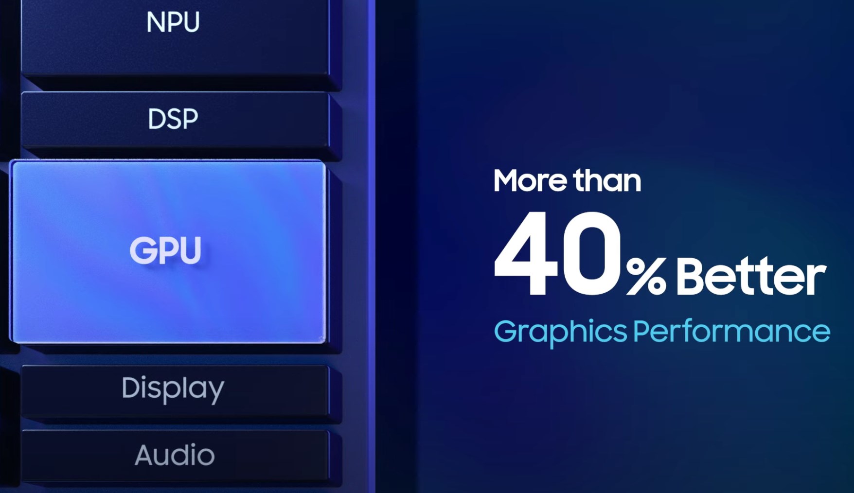
In terms of GPU, we have seen the transition from the Mali-G77MP11 at speeds up to 800MHz to a new Mali-G78MP14 at an unknown frequency. This is generally a predictable implementation boost in terms of the number of cores – 27% more than the exact cores.
What’s interesting here is the fact that Samsung announces 40% better graphics performance. This actually gives me pause and wonder how Samsung achieved such a number. It was supposed to be the Mali-G78 A fairly small generational upgrade with only 10% better performance / W improvements. The process node in the Exynos 2100 was announced as achieving a 20% improvement in energy efficiency. In theory and paper, the new process and GPU IP should improve 32% better / W performance but it is very rare for this theoretical formulation to actually lead to accurate estimates of actual silicon designs, particularly on the GPU side.
So while a 40% performance improvement sounds impressive, it all depends on how much power and how efficient the new Exynos 2100 is – and how well it can maintain those performance numbers in marathon gaming sessions.
The NPU is more powerful

Another big upgrade was found by the new generation NPU. Samsung has upgraded its IP from a dual-core design to a new three-core design, and promises new architectural changes such as trim and weight compression to improve the NPU’s energy efficiency by 2x.
Samsung today announced an AI performance number of 26 TOPS, but that number appears to represent a total across all of the SoC’s computational blocks, including CPU, GPU, NPU, and DSPs, and it compares itself with the Exynos 990’s 15 TOPS number. It already had a 10 TOPS number last year, so there’s a little marketing review going on here, you might want to match the numbers Qualcomm is putting into SoCs. Unfortunately, both companies resort to this obfuscation in actual IP block performance.
More powerful internet service provider – up to 4 sensors at the same time

In terms of multimedia features, Samsung says it has made major improvements to the ISP and DSP of the camera. The new chip supports single sensors up to 200 megapixels, while also connecting up to a total of 6 camera sensors, and at the same time operating 4 of them in parallel. At least in this respect, the new chip offers higher capabilities than Snapdragon 888 that supports up to 3 simultaneous cameras only.
Samsung updated the video decoder and MFC block decoder (multi-format codec) to support up to 8K60 video decoding, although the encoder remained at 8K30 / 4K120. What’s interesting here is that Samsung now supports AV1 decoding, making it the second chip in the mobile market after MediaTek’s Dimensity 1000 to support the new feature.
Integrated 5G modem
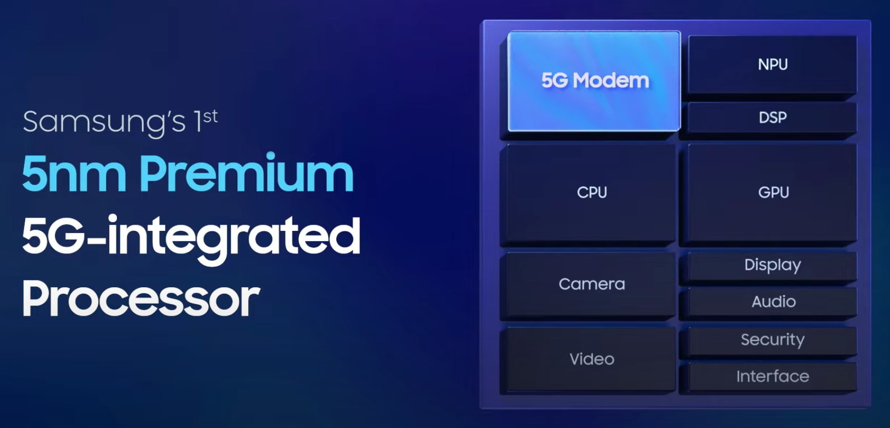
Finally, the new platform is again a new interconnected design, reintegrating a 5G modem on the same silicon mold, which promises some gains in energy efficiency and allows for better PCB space utilization. The actual modem itself doesn’t seem to have seen noticeable changes in features compared to the Exynos 5123 standalone modem – but that’s probably because it was really premium in terms of supporting all new technologies like 5G sub-6GHz and mmWave connectivity.
In the announcement video, Samsung confirmed that mmWave deployments are increasing in 2021, and that we will see more Exynos powered devices using mmWave. This would be interesting as we have yet to see Samsung’s mmWave antennas on the market, even though the company In 2019 That they have multiple generations of these designs.
5nm process node
Finally, Samsung revealed that the new Exynos 2100 is manufactured on Samsung’s 5nm process node, which achieves either a 10% increase in clock frequencies, or a 20% reduction in power at the same frequency. Last year, we suspected Samsung’s 7nm process node was Anywhere between 20 and 25% is less energy efficient From TSMC’s latest N7P contract, so basically we expect the new process to only catch up in terms of energy efficiency, with newer TSMC 5nm SoCs like Like the Apple A14 And the Kirin 9000 still has a remarkable practical node leadership.
Positive messages, good expectations
Today’s launch event was very positive in terms of tone and overall enthusiasm on the part of Samsung, announcing famous phrases like “Exynos is back” and during a presentation admitting that the previous generation of SoCs had problems. I think that’s a big change of messaging from the company, and at least on paper the new Exynos 2100 appears to be very competitive. I hope that the actual matter also translates into actual products, as in a few weeks the new Galaxy S21 series will feature the new Exynos chipset for the first time.
Related reading:

“Загальний ніндзя в соціальних мережах. Інтроверт. Творець. Шанувальник телебачення. Підприємець, що отримує нагороди. Веб-ботанік. Сертифікований читач”


